A side-by-side comparison showing BR100’s specs against NVIDIA’s A100.
Introduction to Biren Technology AI Chips and Their Origins
Biren Technology, whose full name is Shanghai Biren Intelligent Technology Co., Ltd., is a leading Chinese AI chip manufacturer. They founded it in 2019, which was the time when technological competition between China and the US reached its peak. The company aims to design high-performance graphics processing units (GPUs) and other AI chips for data centers. People also call it the NVIDIA of China as it attempts to challenge the dominance of NVIDIA. Talking about its founder and key people, Michael Zhang founded Biren and serves as the founder and CEO of the company.
According to some reports, co-founder Xu Lingji has recently left the company. The company consists of former employees of various giant tech companies such as NVIDIA AMD Huawei and Alibaba. Which provides it with a strong technical team. This experienced team is helping the company to develop complex AI chips. Also, the business model of the company is that Biren is a fabless semiconductor company. This means that they design and develop the chips. But do not produce them themselves. Instead, foundries like Taiwan Semiconductor Manufacturing Company (TSMC) produce them. This model gives them the freedom to focus more on research and development (R&D). Which is a key factor in the semiconductor industry.
Biren Technology AI Chips: BR100 and BR104 Specifications and Features
The most important product of Byren is the BR100 GPU. It is designed for AI training and high-performance computing (HPC) in data centers. Byren Features Number of Transistors The BR100 has 77 billion (77B) transistors. Which makes it a very complex and powerful chip. This compares NVIDIA’s A100 (54.2 billion). Also, TSMC manufactures it using the 7nm process.And Performance The company claims that this BR100 can compete with NVIDIA’s H100 and A100 chips in some workloads. INT8 Performance It offers INT8 performance of 2048 TOPS (Tera-Operations Per Second). FP32 Performance Up to 256 TFLOPS (Tera-Floating Point Operations Per Second) Memory.
It has 64GB HBM2E memory with a bandwidth of 1.64 TB/s. Available in OAM (OCP Accelerator Module) form factor. Which consumes up to 550W of power Interconnection The BR100 has 8-way BLink™ technology. Which allows connecting up to 8 BR100 GPUs in a single system. And the features of BR104 are that BR104 is a smaller version of the BR100. It also offers 128 FP32 TFLOPS or 1 INT8 PetaFLOPS performance. It has memory 32GB HBM2E memory with a bandwidth of 819 GB/s. Form factor It comes as a PCIe card and consumes up to 300W of power. Its significance is that These chips are an important step towards China’s technological self-reliance. The BR100 is built on an independently developed architecture and uses chiplet technology which is an advanced method in semiconductor design.
Introduction and birth of Biren Technology
Biren Technology, whose full name is Shanghai Biren Intelligent Technology Co., Ltd., is a leading Chinese AI chip manufacturer. It was founded in 2019, which was the time when technological competition between China and the US reached its peak. The company aims to design high-performance graphics processing units (GPUs) and other AI chips for data centers. People also call it the NVIDIA of China as it attempts to challenge the dominance of NVIDIA. Talking about its founder and key people, Michael Zhang founded Biren and serves as the founder and CEO of the company.
According to some reports, co-founder Xu Lingji has recently left the company. The company consists of former employees of various giant tech companies such as NVIDIA AMD Huawei and Alibaba. Which provides it with a strong technical team. This experienced team is helping the company to develop complex AI chips. Also, the business model of the company is that Biren is a fabless semiconductor company. This means that they design and develop the chips. But do not produce them themselves. Instead they get them produced by foundries like Taiwan Semiconductor Manufacturing Company (TSMC). This model gives them the freedom to focus more on research and development (R&D). Which is a key factor in the semiconductor industry.
Byren’s main products BR100 and BR104
The most important product of Byren is the BR100 GPU. It is designed for AI training and high-performance computing (HPC) in data centers. Byren Features Number of Transistors The BR100 has 77 billion (77B) transistors. Which makes it a very complex and powerful chip. This is compared to NVIDIA’s A100 (54.2 billion). Also manufacturing process It is made using TSMC’s 7nm process. And Performance The company claims that this BR100 can compete with NVIDIA’s H100 and A100 chips in some workloads. INT8 Performance It offers INT8 performance of 2048 TOPS (Tera-Operations Per Second). FP32 Performance Up to 256 TFLOPS (Tera-Floating Point Operations Per Second) Memory It has 64GB HBM2E memory with a bandwidth of 1.64 TB/s. Available in OAM (OCP Accelerator Module) form factor.
Which consumes up to 550W of power Interconnection The BR100 has 8-way BLink™ technology. Which allows connecting up to 8 BR100 GPUs in a single system. And the features of BR104 are that BR104 is a smaller version of the BR100. It also offers 128 FP32 TFLOPS or 1 INT8 PetaFLOPS performance. It has memory 32GB HBM2E memory with a bandwidth of 819 GB/s. Form factor It comes as a PCIe card and consumes up to 300W of power. Its significance is that These chips are an important step towards China’s technological self-reliance. The developers built the BR100 on an independently developed architecture and used chiplet technology, which is an advanced method in semiconductor design.
Funding Boost and IPO Plans for Biren Technology AI Chips in Hong Kong
Byren Technology recently completed a new funding round of approximately 1.5 billion yuan (approximately $207 million USD). This funding is mainly from state-affiliated investors from China. With this funding, the company has begun preparing for its initial public offering (IPO) in Hong Kong. Funding Purpose Research and Development (R&D) This capital will be used to develop new generation chips and improve existing products. Product Development This will help the company expand its range of products and meet the changing needs of the market. Facing sanctions The funding will help the company deal with the effects of US sanctions and strengthen its supply chain.
Hong Kong IPO Plans Timeline According to sources, Byren is preparing to file for a listing in Hong Kong, possibly by August, in the third quarter (Q3) of this year. Also changed location Byren previously filed documents to be listed on Shanghai’s STAR Market but now his focus has shifted to Hong Kong. The main reason for this is the strict regulatory requirements for listing in land China. Especially for loss-making companies. In Hong Kong, the rules are a little more flexible. Which makes listing easier for companies like Biren. Importance of IPO This IPO will help Biren raise a large amount of capital which is necessary for growth in a capital-intensive industry like semiconductors. It will bring the company to the public platform, increasing its credibility and global reputation.
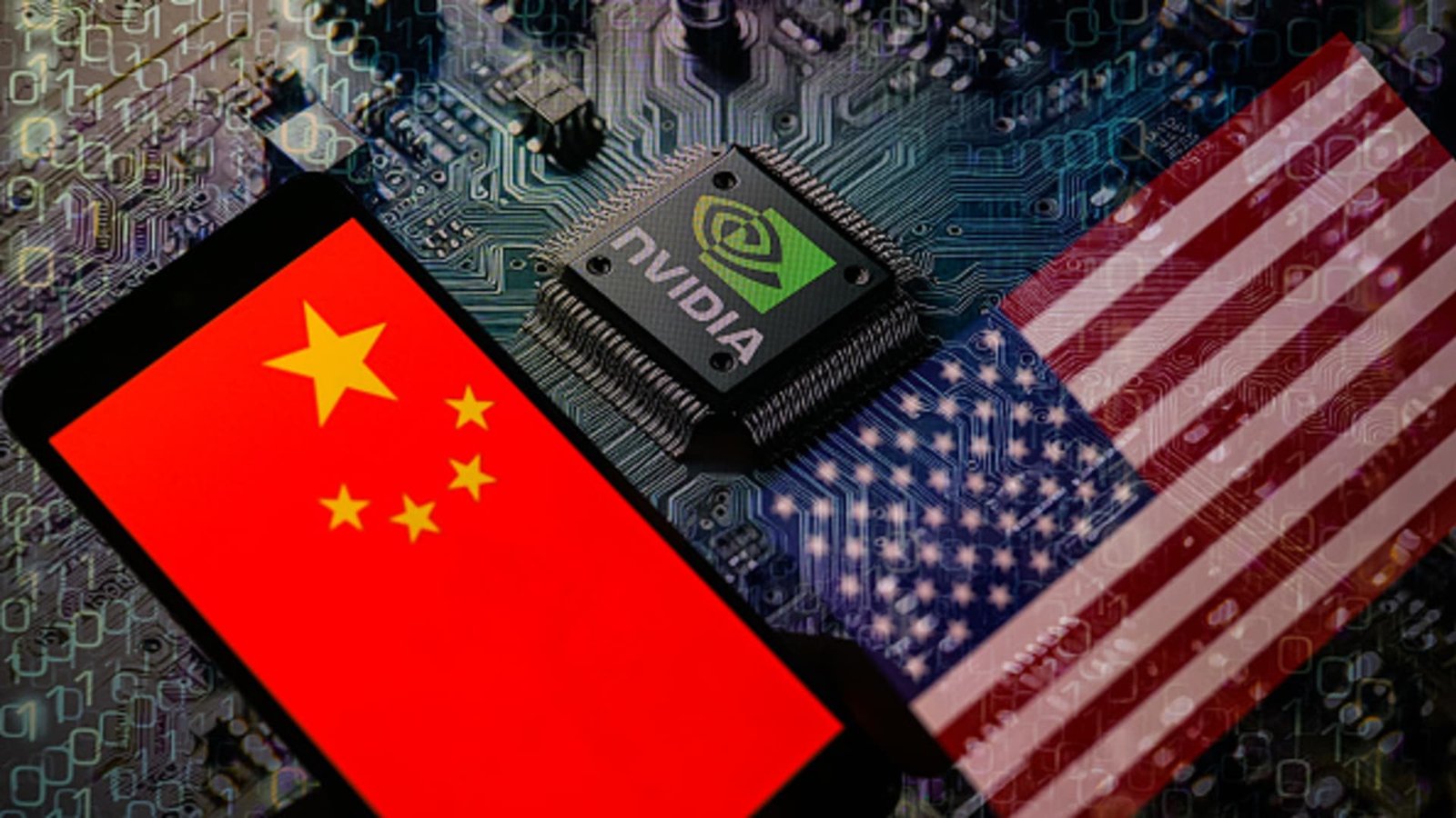
The Future of Chinese AI Chips and Biren Technology’s Strategic Role
In October 2023, the US government added Biren Technology to its Entity List. This means that US companies and their affiliates need a license to sell advanced chips and technology to Biren. Impact of sanctions as well as production disruptions Biren which relied on foundries like TSMC is now facing difficulties in getting its advanced chips produced. TSMC has to comply with US sanctions, which has halted production for Byren These technical barriers.
The sanctions have also prevented Byren from accessing advanced US software and design tools (EDA). Which are necessary for chip design. Revenue and losses Byren is suffering losses due to the sanctions and its revenue is limited. The company’s revenue in 2024 was 400 million yuan and it is still running in losses. And Byren’s response and challenges To deal with domestic supply chain restrictions, Byren is now considering working with domestic Chinese foundries such as SMIC. However, Chinese foundries still lag behind TSMC in 7nm or advanced processes which may affect the quality and performance of Byren’s chips. Chip redesign According to reports, Byren has modified some of its chips so that they fall below the performance threshold of the US sanctions. This is a temporary solution but it can help the company continue business to some extent.
Future of China’s AI chip industry and role of Biren
US sanctions have forced China to move rapidly towards its semiconductor self-sufficiency. Biren is at the forefront of this effort. Future prospects and growing demand There is a huge growth in AI applications in China such as data center cloud computing and autonomous driving. Which is increasing the demand for AI chips. Also government support The Chinese government is investing heavily in AI and the semiconductor industry. Startups like Biren are getting government funds and policies that help them in research and development. The importance of Hong Kong now is that it has become an important financial center for Chinese companies that want to stay away from US exchanges.
Conclusion
Biren Technology’s new funding and Hong Kong IPO plan is an important step in China’s mission of technological self-sufficiency. The company is facing major challenges due to US sanctions. But it is trying to face these challenges by focusing on domestic capital and market. Byron’s future is crucial to the success of China’s semiconductor industry. And if the company is able to improve its technology and solve production problems, it could become a significant player in the global AI chip market. This is not just the story of one company. It is also a symbol of a larger technology war between China and the US.